Optical transmission hardware integration one-stop service provider

Views: 7 Author: Ada Ru Publish Time: 2021-11-23 Origin: Site
PLC chips are generally made on six materials, they are: lithium niobate (LiNbO3), the waveguide is formed by diffusing Ti ions on the lithium niobate crystal to form a waveguide, the waveguide structure is diffusion type; III-V group semiconductor compound, waveguide InP is called the bottom and lower cladding layer, InGaAsP is the core layer, InP or InP/air is the upper cladding layer, and the waveguide structure is a buried ridge or ridge; SOI (Silicon-on-Insulator), The waveguide is fabricated on an SOI substrate. The materials for the bottom, undercladding, core and upper cladding are Si, SiO2, Si and air respectively. The waveguide structure is ridge-shaped, as well as polymer (Polymer) and silicon dioxide (SiO2). , Glass ion exchange, etc.

There are no problems with fiber-to-the-home (FTTH) network technology at present, but whether it can rapidly develop and popularize in my country, in addition to policy, the most important and critical point is to reduce the cost of each link of the network. The PLC optical splitter is one of the core devices in the FTTx network, and low cost is its important technical development goal. It can be seen from the technology, cost and characteristics of the optical waveguide materials given in the above table that silicon dioxide, polymers and glass are the most suitable for making PLC chips. The following briefly introduces three PLC chip technologies with the lowest cost and the easiest industrial realization:
(1) Polymer (spin coating-etching)
The polymer waveguide is based on a silicon wafer, and polymer materials with different doping concentrations are used as the core layer. The waveguide structure is a buried rectangle. Polymer waveguides and devices have a simple manufacturing process and low price. If they are photosensitive, the manufacturing cost is lower (theoretical value), and they have great development prospects. The problem is that the cost of fluorinated materials is high; the aging doubts and loss will be relatively high; the stability of the product needs to consider its influence. At present, only Shanghai NITTA company has optical splitter products made with this chip.
(2) Silica
The silicon dioxide waveguide is called a silicon wafer as the base, and differently doped SiO2 materials are used as the core and cladding. The waveguide structure is a buried rectangle. Silicon-based silicon dioxide light wave technology is a new technology developed in the 1990s, and it is relatively mature abroad. Its manufacturing processes include flame hydrolysis (FHD), chemical vapor deposition (PECVD, developed by NEC in Japan), plasma CVD (developed by Lucent in the United States), porous silicon oxidation method and melt-gel (Sol-gel) Wait. This kind of waveguide and loss is very small, about 0.05dB/cm or less. Foreign countries have developed 60 AWGs and 132 AWGs using this waveguide. At present, flame hydrolysis (FHD) and chemical vapor deposition (PECVD) are widely used to grow multilayer silicon dioxide materials, and dry etching technology is used to complete waveguide etching.
Its advantage is that it has very good physical and chemical stability technology, high device integration and low cost. At the same time, it has good compatibility with optical fiber, low transmission loss, mature technology (mainly dependent on the import of equipment), stable and reliable products, and theoretically can also make other PLC devices such as AWG. This process technology is currently the mainstream technology for the manufacture of chip products, and is widely adopted internationally. The problem is that the equipment investment is high, the maintenance cost is high, and the raw material requirements are high (all imported materials are used); there are only a few domestic research institutes and universities on-line experimental equipment and Wuhan Guangxun Technology’s silica PLC process line, which are not available for use. Industrial scale production equipment. This technology and manufacturing are basically monopolized by foreign manufacturers such as South Korea and Japan.
(3) Glass base (ion exchange)
Glass waveguide is a waveguide formed by diffusing Ag ions on a glass material, and the waveguide structure is a diffusion type. The advantage is that the process is relatively simple, the equipment is relatively simple, the total investment is not large, and the product is relatively stable and reliable. The manufacturing process of the glass optical waveguide is divided into five steps: 1) Sputter a layer of aluminum on the glass substrate as a mask layer during ion exchange; 2) Carry out photolithography, and protect the required waveguide pattern with photoresist 3) Use chemical etching to remove the aluminum film on the upper part of the waveguide; 4) Put the masked glass substrate into a mixed solution containing Ag+-Na+ ions, and perform ion exchange at an appropriate temperature to increase Ag+ ions Refractive index to obtain a channel-type optical waveguide; 5) Apply an electric field to the channel-type optical waveguide to drive Ag+ ions to the depths of the glass substrate to obtain a buried glass optical waveguide. The main problems of this technology: ① Will it become the mainstream technology in the future, and some experts have doubts? ② Because there is no large-scale commercialization and industrial production, the actual process stability of the product needs to be verified.
The above-mentioned technology is currently only produced by Teemphotonics in France and Colorchip in Israel. It is said that the original E-TeK company has this technology, but the specific details are unknown and cannot be verified. The research group of Professor Wang Minghua from the Department of Information and Telecommunications of Zhejiang University in China began to cooperate with communication companies to develop splitters based on glass ion exchange optical waveguides and achieved certain results a few years ago. Their advantage is that the key technology is fully mature, all raw materials do not need to be imported, which can be fully satisfied in China, and they have developed optical splitters with performance indicators that reach the level of similar foreign products, and all their intellectual property rights are their own. At present, the commercial and industrialized technologies have not yet fully passed the barriers, and intermediate tests must be carried out, and various technical parameters must be further improved. Therefore, from the perspective of domestic industrialization, there is a considerable gap between PLC chip manufacturing technology and foreign countries, and the process of technology practicality and industrialization still needs a long way to go.
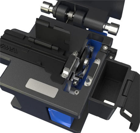
The encapsulation of PLC splitter means to align each light guide path (ie waveguide path) on the planar waveguide splitter with the optical fibers in the optical fiber array one by one, and then glue them with a specific glue (such as epoxy glue) Technology together. Among them, the alignment accuracy of the PLC splitter and the optical fiber array is the key to this technology. The packaging process includes operations such as coupling alignment and bonding. The coupling alignment between PLC splitter chip and optical fiber array is manual and automatic. The hardware they rely on mainly includes six-dimensional precision fine-tuning frame, light source, power meter, microscopic observation system, etc., and the most commonly used is automatic alignment , It forms closed-loop control through optical power feedback, so the docking accuracy and docking coupling efficiency are high.